Introduction
One of the arcade classics is Lady Bug, a labyrinth game similar to Pacman which adds some features to the gameplay like swing walls and a bonus system that challenges the player’s ability to combine the hunt for dots with a precise timing.
This project takes the old-time PCB circuits and packs it into modern FPGA devices, virtualizing the whole hardware and moving it away from aging silicon chips to virtually any hardware platform of today and the future. On the other hand, implemeting the game hardware in an FPGA can achieve the most accurate level of emulation, including even quirks that breed in the circuits of the original design like graphic glitches or off-field distortions. The next (and ultimate) level of accuracy is to rebuild the hardware with real chips resulting in a clone board.
Apart from Lady Bug, some other games targetted the same PCB hardware: Cosmic Avenger and Dorodon. They also run on the design of this project by simply replacing the ROMs.
Content
This project recreates all circuits that are found on the original arcade PCB including CPU, RAM, character and sprite graphics and sound generation. Some memory elements like RAM and PROMs are embedded inside the design while the program, character and sprite ROMs are located outside of the design. This is mainly due to the resource requirements of these ROMs that cannot be satisfied with low-range FPGAs.
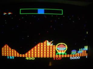
Actual photo taken by compiling and running the code here. This is Cosmic Avenger.
Internal components of the Lady Bug machine
CPU Unit
- Z80 CPU – T80 core from opencores.org / fpgaarcade.com
Copyright (c) 2001-2002 Daniel Wallner (jesus at opencores.org)
Ver 300 started tidyup, MikeJ March 2005
Latest version from www.fpgaarcade.com (original www.opencores.org) - 4 kByte CPU RAM
- General purpose I/O for joysticks and DIP switches
- Timers for left and right coin chutes
- Decryption PROMs (256 Bytes in total)
Sound Unit
- Two instances of the SN76489 sound generator
- Audio mixer
- Clock generator – operates with main 20 MHz clock (external or PLL)
- Reset generator – requires power-on reset capability of FPGA
Video Unit
- Video timing generator
- Character graphics circuit, including 1 kByte tile data RAM and 512 Byte color RAM
- Sprite graphics circuit, including 1 kByte sprite data RAM, 2 kByte sprite VRAM, 32 Byte sprite color look-up PROM and 32 Byte sprite control PROM
- Character and sprite graphics color mixer with RGB loop-up PROMVideo Unit
External components are:
- CPU program ROM – 24 kByte
- Character graphics ROM – 8 kByte
- Sprite graphics ROM – 8 kByte
- RGB DACs
- Audio DAC
Arcade Machine Interfaces
The external components are attached via several interfaces to the Lady Bug machine:
- Clock Input: Base clock of 20 MHz.
- Reset Input: Active low external reset input. Debounced and extended by the internal reset unit (originally an NE555 in monostable mode).
- Control Interface:
- Player 1 – 4-way joystick, two action buttons and a select button
- Player 2 – 4-way joystick, two action buttons and a select button
- Left coin chute trigger
- Right coin chute trigger
- Tilt trigger
- DIP Switch Interface: Two blocks consisting of 8 switches each. Their assignment is specific to the game.
- RGB Video Interface:
- 2 bit wide channels for red, green and blue video information
- Composite synchronization output
- Audio Interface
- 8 bit digital audio sound output
- 1 bit Delta-Sigma DAC sound output
- CPU ROM Interface: Address and data buses for 24 kByte of CPU program ROM
- Character ROM Interface: Address and data buses for 2 x 4 kByte of character graphics data ROM
- Sprite ROM Interface: Address and data buses for 2 x 4 kByte of sprite graphics data ROM
Control
Both the axis and button inputs for the joystick ports are low active as is the tilt input. In contrast, the coin chute triggers are high active. A trigger impulse at the latter ones is shaped on the original PCB by NE556 timers, probably to suppress glitches that would generate multiple coin events otherwise. This shaping is also done although it might be not necessary for a “clean” digital design environment.
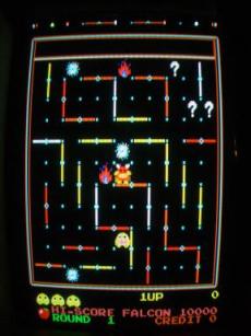
Actual photo taken by compiling and running the code here. This is Dorodon.
External Memory
Especially the ROM interfaces could be a challenge when implementing the FPGA Lady Bug machine on small development boards. At a first glance, it seems that three separate external ROMs have to be attached to suit these requirements. Thanks to the clocking system, it is possible to supply the ROM data from a single 8 bit wide memory by multiplexing all three data channels. The external memory has to be capable of providing 8 bits of data in parallel at a clock frequency of 20 MHz. For details refer to the three components in src/board/misc:
rom_dispatcher_8.vhd
standard data path multiplexer for external 8 bit memoryrom_dispatcher_16.vhd
wrapper to accommodate 16 bit memoryrom_ram_dispatcher_16.vhd
combined ROM and CPU RAM multiplexer
The first two designs simply feed the CPU, character and sprite ROM interfaces from any external memory (ROM or RAM). The latter design enables implementation of the FPGA Lady Bug project in devices which contain too few internal RAM resources. One example is the Spartan IIe 300 which lacks exactly 1 BRAM to implement all memory arrays inside the device. By setting the generic external_ram_g to 1, the 4 kByte CPU RAM is removed from the FPGA and has to be attached via a separate memory interface to ladybug_machine.vhd. This additional port is served by rom_ram_dispatcher_16.vhd which multiplexes all four data channels (3 ROMs + 1 CPU RAM) to a single 16 bit wide external RAM. This combined approach is optional as it is always possible to feed the 3 ROMs from one external memory (with the help of rom_dispatcher_x) and the CPU RAM from a separate external RAM device.
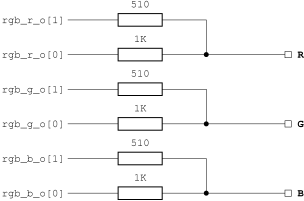
RGB Video
The digital information for the three RGB channels have to be converted to analog voltages by three DAC circuits, each of them consists of simple resitors. See the following figure for a proposal on how to build them.
The better approach is to use a professional DAC circuit like found on the Zefant Mini-ITX board. This one offers a VGA interface to a standard PC monitor. Three video DAC channels can be fed with 8-bit wide color information each. The drawback is that the simple RGB video information has to be brushed up to suit the VGA standard. A scan doubler is used here to double the pixel rate towards the VGA monitor although the VDP inside the console core still outputs RGB video signals.
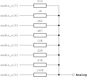
Digital Audio
The digital audio information is supplied via an 8 bit wide signed vector ranging from -128 to 127 (as defined in numeric_std package). It depends on the DAC implementation on your board whether this value can be used as it is or some post processing is needed. On the JOP board, I use two DAC implementations in parallel. First is a DAC built with resistors. This requires to add an offset of 128 to the signed value to obtain positive audio data. Refer to the following picture for the discrete DAC.
Next is a delta-sigma DAC implementation. This one requires a minimum number of external components but adds some logic in the FPGA. For a detailed discussion of delta-sigma DACs refer to Xilinx’ application note XAPP154. The external circuit is shown in the next figure.
Please keep in mind that the output of these circuits can reach the full VCCIO level of the FPGA device. Make sure to match the level to the requirements of the following input.
Again, the Zefant Mini-ITX board provides a professional solution here as well. It contains an AC97 compatible codec chip that handles all the audio stuff. You “simply” have to supply an AC97 audio stream. Fortunately, the AC97 controller core from opencores.org has proven to be versatile enough to allow ad-hoc generation of such a stream. All required design instances are included in the project release.
Porting to a Specific Platform
Two separate issues have to be considered when the FPGA Lady Bug design is ported to different platforms.
At first, an additional top level design has to be generated that wraps the FPGA Lady Bug machine and embeds it in the environment of the given FPGA board. All related design files should be stored in directory src/board/<board>. There you will find the implementations for the JOP.design Cyclone board, the BurchED B5-X300 board and Simple-Solutions‘ Zefant-XS3 board.
Next, the technology dependent parts of the design have to be resolved. These design units are located in directory src/tech/<technology>. The following sections describe the components in detail.
Power-on Reset Module
The power-on reset module in ladybug_por.vhd uses device specific features to generate a reset signal upon power-on (or start of operation after device configuration). Consult the documentation of the FPGA device family on how to implement such functionality.
RAM Macros
All RAM wrappers simply instantiate a single RAM macro. For Altera’s Cyclone family and Xilinx’ Spartan2e family a parametrizable generic RAM instance (pure RTL code) is used here, which is automatically translated to device specific RAM blocks. Other device families might need dedicated macro instantiations to implement the required memory configurations.
| Name | Memory Layout | Design File |
|---|---|---|
| CPU RAM | 4 k x 8 | ram_4kx8.vhd |
| Character Data RAM | 1 k x 8 | ram_1kx8.vhd |
| Character Color RAM | 1 k x 4 | ram_1kx4.vhd |
| Sprite Data RAM | 1 k x 8 | ram_1kx8.vhd |
| Sprite VRAM | 1 k x 4 | ram_1kx4.vhd |
PROM Macros
Similar to the RAM wrappers, several PROM wrappes exist that instantiate a ROM macro. The common approach is to use RTL VHDL code to implement the ROMs and let the implementation tool turn the code into a device specific memory macro. Automatic generation of the RTL code is done with the hex2rom utility provided in this release (written by Daniel Wallner). Refer to roms/hex/Makefile for the commands required to build the RTL ROMs. This method has been tested with Quartus II 5.0/6.0 and Xilinx ISE 7.1/8.1 so far.
Depending on the device characteristics and the design software, a different approach has to be taken to preload the ROM macros with the data of the initialization files. For historical reference, PROM wrappers are kept for Altera’s Cyclone family utilizing the parametrizable generic RAM macro altsyncram with an additional hex file containing the PROM data.
| Name | Memory Layout | Design File | Data File |
|---|---|---|---|
| RGB Look-up PROM | 32 x 8 | prom_10_2.vhd |
10-2.bin |
| Sprite Color Look-up PROM | 32 x 8 | prom_10_1.vhd |
10-1.bin |
| Sprite Control PROM | 32 x 8 | prom_10_3.vhd |
10-3.bin |
| Decryption PROM, lower | 256 x 4 | prom_decrypt_l.vhd |
decrypt_l.bin |
| Decryption PROM, upper | 256 x 4 | prom_decrypt_u.vhd |
decrypt_u.bin |
ROM Memory Data
Each game consists of several binary files which were dumped from the original (E)PROM chips on the PCB. This section describes how they have to be arranged to fit the requirements of the FPGA Lady Bug machine. As there is no standard naming scheme for the ROM files, they are referred to with the names used inside the MAME ROM sets.
| Generic Name | Lady Bug | Cosmic Avenger | Dorodon | Pos |
|---|---|---|---|---|
cpu1.bin |
lb1.cpu |
1 |
dorodon.0 |
C4 |
cpu2.bin |
lb2.cpu |
2 |
dorodon.1 |
D4 |
cpu3.bin |
lb3.cpu |
3 |
dorodon.2 |
E4 |
cpu4.bin |
lb4.cpu |
4 |
N/A |
F4 |
cpu5.bin |
lb5.cpu |
5 |
N/A |
H4 |
cpu6.bin |
lb6.cpu |
6 |
N/A |
J4 |
sprite_l.bin |
lb8.cpu |
8 |
dorodon.4 |
L7 |
sprite_u.bin |
lb7.cpu |
8 |
dorodon.3 |
M7 |
char_l.bin |
lb9.vid |
9 |
dorodon.5 |
F7 |
char_u.bin |
lb10.vid |
0 |
dorodon.6 |
H7 |
10-1.bin |
10-1.vid |
k9.bpr |
dorodon.bp1 |
F4 |
10-2.bin |
10-2.vid |
t8.bpr |
dorodon.bp0 |
K1 |
10-3.bin |
10-3.vid |
h9.bpr |
dorodon.bp2 |
C4 |
decrypt_l.bin |
N/A - use dummy |
N/A - use dummy |
dorodon.bp3 |
|
decrypt_u.bin |
N/A - use dummy |
N/A - use dummy |
dorodon.bp4 |
Note that the ROM set for Dorodon contains only three images for the CPU ROM. Each file is twice the size of a file for Lady Bug for example, resulting in the same CPU ROM memory size of 24 kByte. The remaining files cpu4.bin, cpu5.bin and cpu6.bin are not required therefore.
The two 16 bit wide ROM data buses for character and sprite data are fed by the two ROMs *_l.binand *_u.bin in parallel. The *_l.bin file has to be connected to bits (7 downto 0) while the *_u.bin file is connected to bits (15 downto 8).
Only Dorodon actually requires decryption PROMs. Use the dummies provided in the respective directories under roms for Lady Bug and Cosmic Avenger.
In case you work on Linux or another UNIX derivate, you can use the provided Makefiles and scripts in the roms directory tree. Simply copy the ROM set into the empty directory and from within roms issue for example
$ make ladybugYou will need the srecord utilities for binary to hex conversion (not required when RTL PROMs are used) and the automated packaging of the ROM image (always required for the *_dispatcher modules).
Resource Usage
Following is the flow summary for an Altera Cyclone device:
+------------------------------------------------------------------------+
; Flow Summary ;
+-------------------------+----------------------------------------------+
; Flow Status ; Successful - Fri Oct 28 23:47:54 2005 ;
; Quartus II Version ; 5.0 Build 168 06/22/2005 SP 1 SJ Web Edition ;
; Revision Name ; jop_ladybug ;
; Top-level Entity Name ; jop_ladybug ;
; Family ; Cyclone ;
; Device ; EP1C12Q240C8 ;
; Timing Models ; Final ;
; Met timing requirements ; Yes ;
; Total logic elements ; 3,275 / 12,060 ( 27 % ) ;
; Total pins ; 138 / 173 ( 79 % ) ;
; Total virtual pins ; 0 ;
; Total memory bits ; 72,320 / 239,616 ( 30 % ) ;
; Total PLLs ; 1 / 2 ( 50 % ) ;
+-------------------------+----------------------------------------------+
Fitting results for a Spartan-IIE 300 (XC2S300EPQ208):
Logic Utilization:
Number of Slice Flip Flops: 1,000 out of 6,144 16%
Number of 4 input LUTs: 3,365 out of 6,144 54%
Logic Distribution:
Number of occupied Slices: 2,008 out of 3,072 65%
Number of Slices containing only related logic: 2,008 out of 2,008 100%
Number of Slices containing unrelated logic: 0 out of 2,008 0%
*See NOTES below for an explanation of the effects of unrelated logic
Total Number 4 input LUTs: 3,485 out of 6,144 56%
Number used as logic: 3,365
Number used as a route-thru: 120
Number of bonded IOBs: 57 out of 142 40%
IOB Flip Flops: 31
Number of Block RAMs: 14 out of 16 87%
Number of GCLKs: 1 out of 4 25%
Number of GCLKIOBs: 1 out of 4 25%
Total equivalent gate count for design: 260,965
CONTROLS
## Controls
### Joystick
Attach joystick to port 1. A second joystick is currently not supported.
### Virtual keyboard
The joystick in port 1 is emulated in parallel using the virtual keyboard:
* Cursor up, down, left, right
* enter -> fire
* space -> bomb
* key 5 -> coin
* key 1 -> start 1
# Acknowledgements
* Original FPGA conversion by Arnim Laeuger
* A-Z80 core by Goran Devic, https://github.com/gdevic/A-Z80
* SN76489 core by Arnim Laeuger
## Video output
R1 and V4 both output 640×480 progressive with 60 Hz on DVI (-A and -D) and HDMI, respectively.
Download
Please read the “README” file for documentation.
IMPORTANT NOTE :
NO ORIGINAL ROM CONTENTS ARE IN THIS DISTRIBUTION. YOU WILL NEED THE ORIGINAL/ALTERNATIVE ROM FILES TO RUN THE LADYBUG GAME
Legal Issues
Redistribution and use in source and synthesized forms, with or without modification, are permitted provided that the following conditions are met:
Redistributions of source code must retain the above copyright notice, this list of conditions and the following disclaimer.
Redistributions in synthesized form must reproduce the above copyright notice, this list of conditions and the following disclaimer in the documentation and/or other materials provided with the distribution.
Neither the name of the author nor the names of other contributors may be used to endorse or promote products derived from this software without specific prior written permission.
Please note:
The copyright of the ROM images is owned by third parties, thus the above does not apply to them. You have to be entitled separately to use the ROM images together with the FPGA Lady Bug design. Owning an original PCB might be ok, but I am not liable for any copyright violations that arise from your use of the FPGA Lady Bug design.
I will ignore any requests for a copy of the ROM images.
THIS SOFTWARE IS PROVIDED BY THE COPYRIGHT HOLDERS AND CONTRIBUTORS “AS IS” AND ANY EXPRESS OR IMPLIED WARRANTIES, INCLUDING, BUT NOT LIMITED TO, THE IMPLIED WARRANTIES OF MERCHANTABILITY AND FITNESS FOR A PARTICULAR PURPOSE ARE DISCLAIMED. IN NO EVENT SHALL THE AUTHOR OR CONTRIBUTORS BE LIABLE FOR ANY DIRECT, INDIRECT, INCIDENTAL, SPECIAL, EXEMPLARY, OR CONSEQUENTIAL DAMAGES (INCLUDING, BUT NOT LIMITED TO, PROCUREMENT OF SUBSTITUTE GOODS OR SERVICES; LOSS OF USE, DATA, OR PROFITS; OR BUSINESS INTERRUPTION) HOWEVER CAUSED AND ON ANY THEORY OF LIABILITY, WHETHER IN CONTRACT, STRICT LIABILITY, OR TORT (INCLUDING NEGLIGENCE OR OTHERWISE) ARISING IN ANY WAY OUT OF THE USE OF THIS SOFTWARE, EVEN IF ADVISED OF THE POSSIBILITY OF SUCH DAMAGE.
See also the file COPYING.