The investigations up to this point remained entirely in the digital domain. Waveforms like the ones shown in the VLM5030 gate-level design validation and lock-step comparison post were derived from the PCM data right before it enters the DAC. This is most suitable to obtain precise information about the cycle behaviour of the design but neglects the final conversion step from digital to the analog output at the DAO pin.
What is the DAC’s transfer function, and most importantly: Is it linear or logarithmic?
DAC architecture
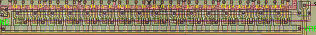
Let’s have a look at the DAC layout.
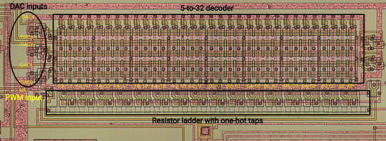
DAC layout
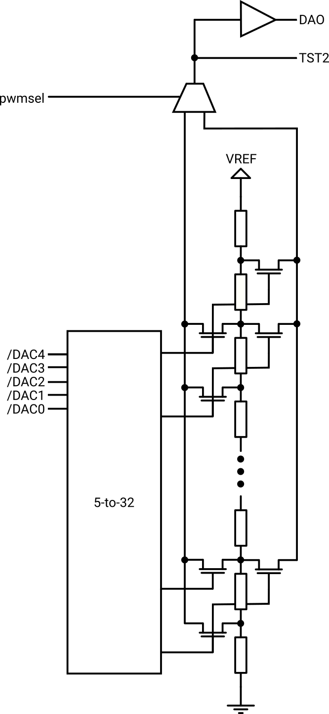
DAC schematic
It’s partitioned into 4 sub-circuits:
- 5 inputs to the DAC (/DAC[4:0])
- The 5-to-32 decoder with a regular ROM-like structure
- 34 resistors chained up (light green rectangles) and tapped by 2x 32 transistors
- A Y-shaped output MUX for the PWM overlay, controlled by sel input
- Output buffer for DAO pin (not visible in the picture above)
The schematic on the right shows the simplified circuit. Note that the PWM overlay is not included.
Based on the schematic we can conclude that the DAC is linear if the values of the 34 resistors are equal. They obviously share the same geometry, but electrical characteristics cannot be obtained from the die shot. Some measurement is needed to clarify details.
Testability considerations
Testing the DAC requires controllability of /DAC[4:0] inputs and observability at the DAC output.
DAC observation in a packaged chip
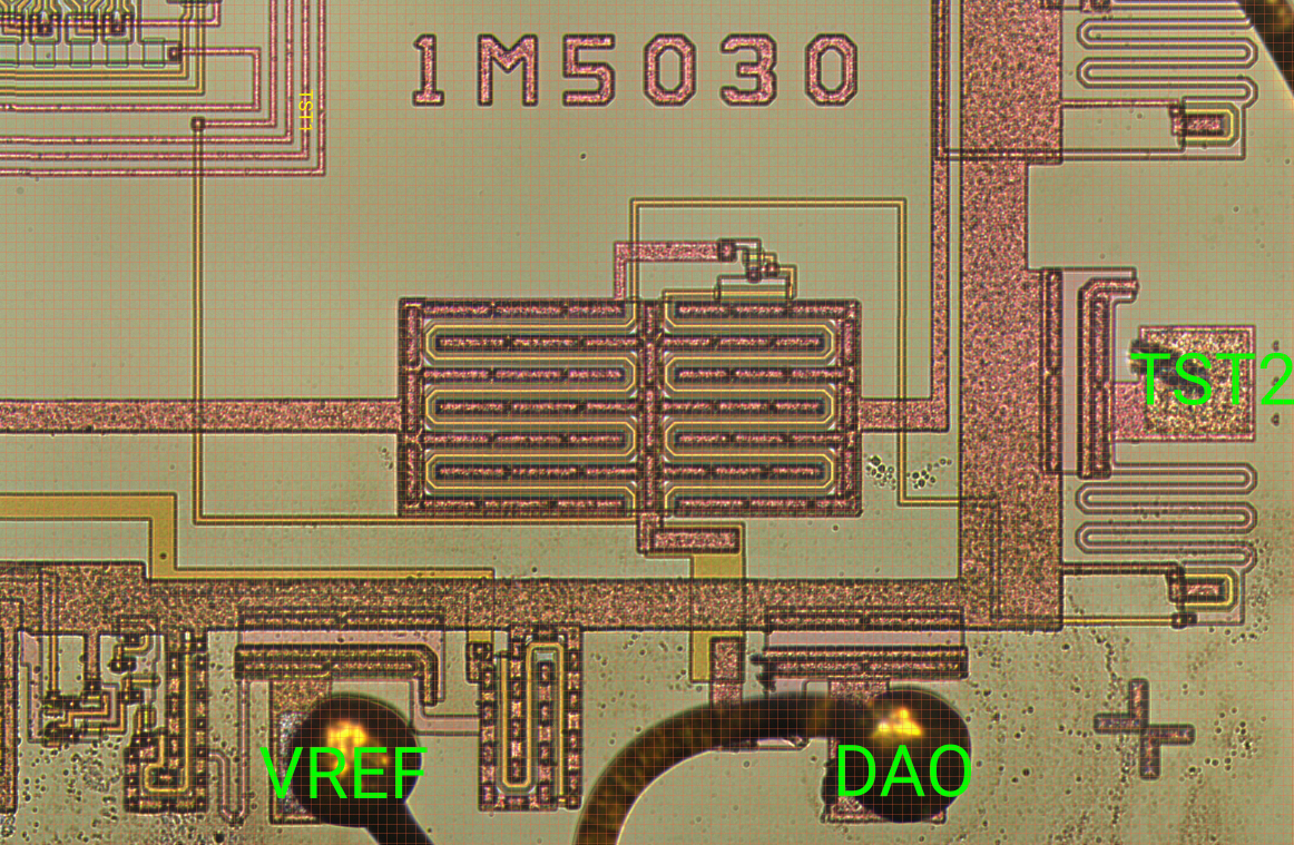
VREF bias, DAO buffered output, TST2 direct output
Starting with the output, there are two options for measuring – at the DAO pin or the TST2 pin. TST2 would be preferable as it provides direct access to the internal node, even allowing to measure resistances directly. Unfortunately, the TST2 pad is not bonded on my chip. The missing bond is also visible in the die shot – there’s only the scrub mark from wafer probing but no bond wire.
DAO is the only feasible observation point.
DAC control with DFT
The situation for control at /DAC[4:0] is more complex since they are internal signals that are computed from the frame parameters. Furthermore, they are highly dynamic, rendering a static output voltage measurement almost unfeasible as a close correlation between input value and output voltage is required.
DFT to the rescue – Sanyo fortunately added test features in the design that come in handy:
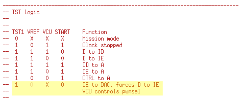
VLM5030 test modes
Enabling TST1 while keeping VREF & START at low activates the DAC test mode that propagates the D[7:0] input bus to /DAC[4:0]. Internally, the frame decoder and register file are bypassed (ID bus) as well as the arithmetic unit that drives onto the IE bus. This test mode also bypasses the register stage for synchronizing the calculated values towards the DAC inputs with the sample rate.
In summary, we get full control over /DAC[4:0] from external pins without the need to sync to any clock!
Measurement
The final measurement setup is straight forward now. A modified FSM inside the test rig activates the DAC test mode and linearly sweeps the DAC inputs while the output voltage is captured at DAO.
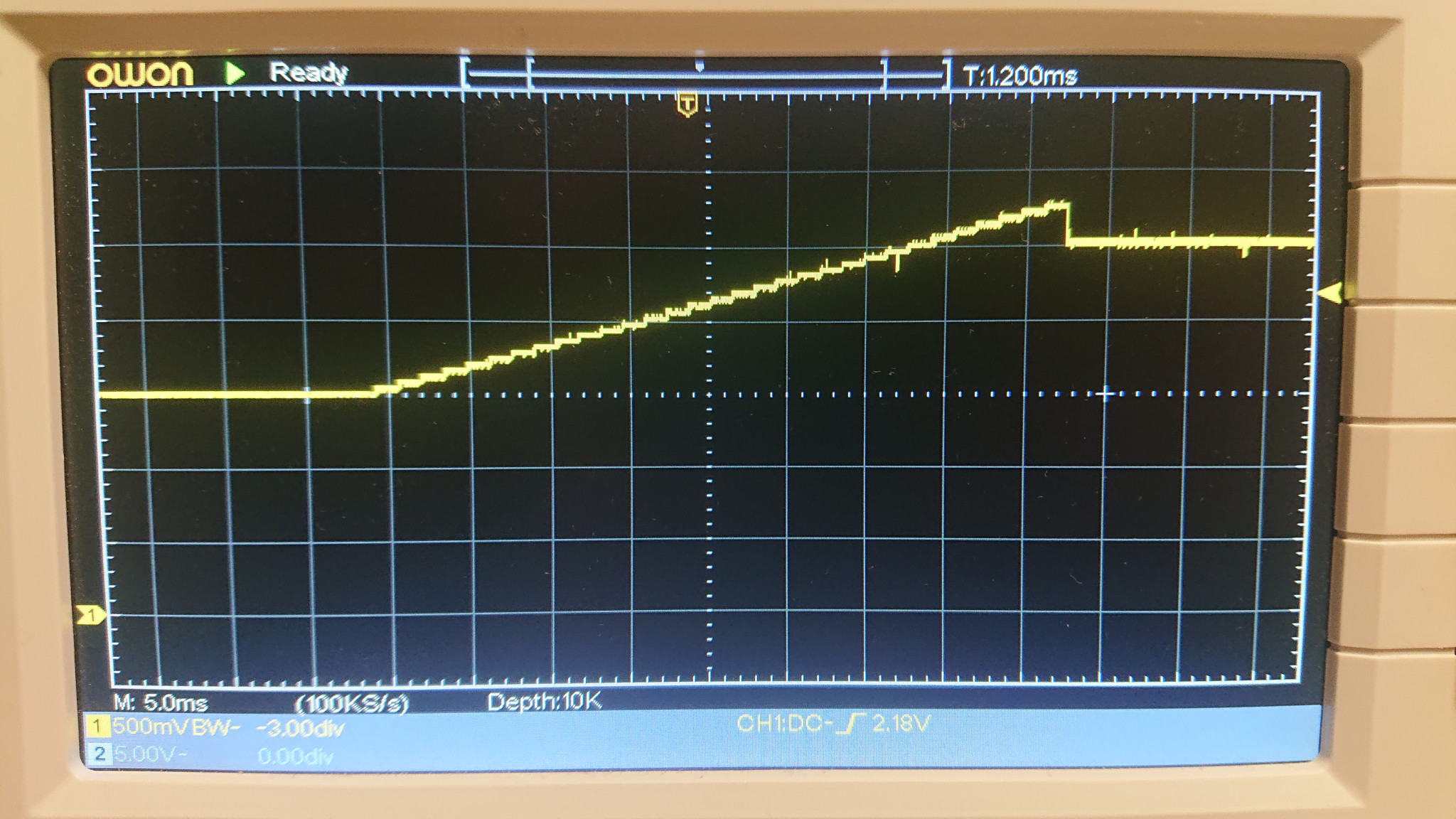
DAC output voltage sweep
The resulting ramp confirms the initial assumption that the transfer function of the DAC is indeed linear.