The technology
We need to set the stage first for this post. The VLM5030 is built from depletion-load NMOS logic. This means there are basically two types of devices:
- Enhancement-mode NMOS transistors for shorting a node to GND (or forwarding voltage between two nodes)
- Depletion-mode NMOS transistors to act as pull-ups to VDD
In addition, there are a total of three layers to connect devices in decreasing order or conductivity:
- Metal (red) for general signal routing and VDD & GND distribution
- Polysilicon (orange) for general signal routing and transistor gates
- Diffusion (transparent) for routing over small distances or of uncritical signals
Layers are interconnected with vias:
- Metal to polysilicon
- Metal to diffusion
A remarkable item is that the VLM5030 doesn’t connect polysilicon directly to diffusion. Consequently, whenever a signal needs to change from polysilicon to diffusion or vice versa, there’s first a via from polysilicon to metal and next to it a second via connecting metal to diffusion. Other chips like the MOS6502 solve this with buried contacts that allow direct connections between polysilicon and diffusion. So Sanyo used a less advanced technology, probably to save on cost per wafer. But it actually helps the tracing task since the layer change is pretty obvious this way.
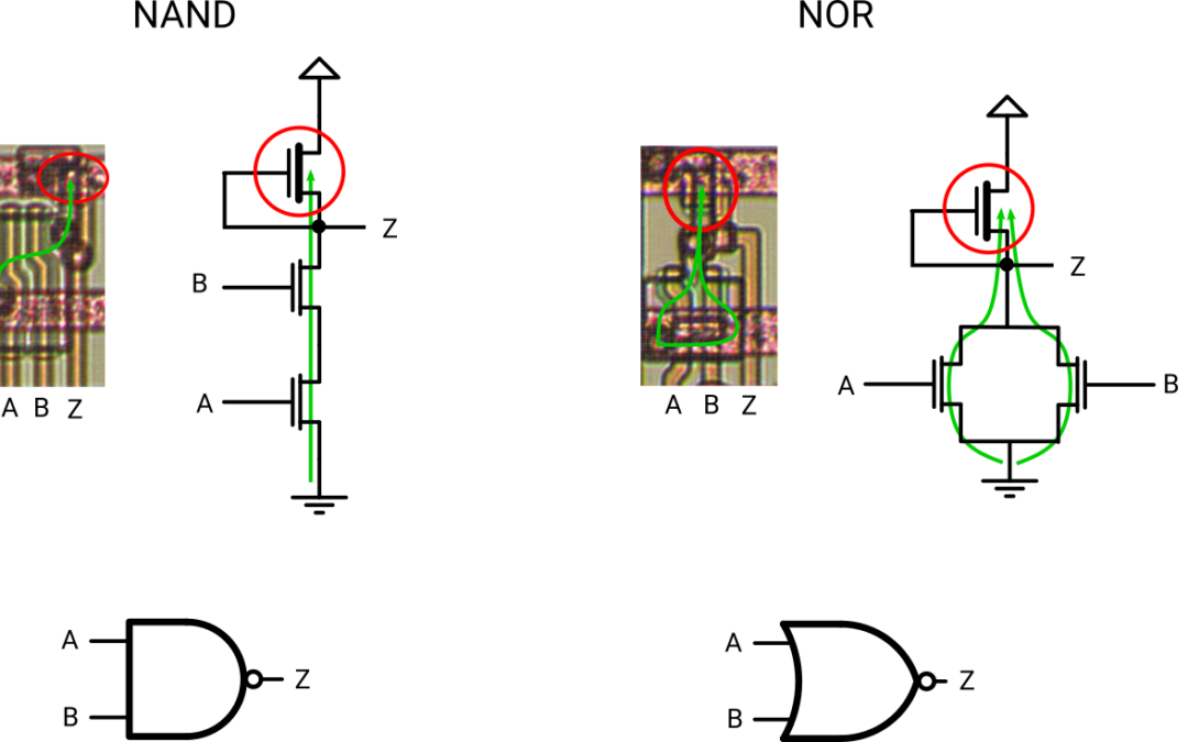
Basic logic gates
To understand which kind of logic gate is built by a particular group of transistors, apply the following basic tracing procedure:
- Start from the GND metal
- Follow the path(s) along the enhancement-mode transistors
- Stop at the pull-up transistor
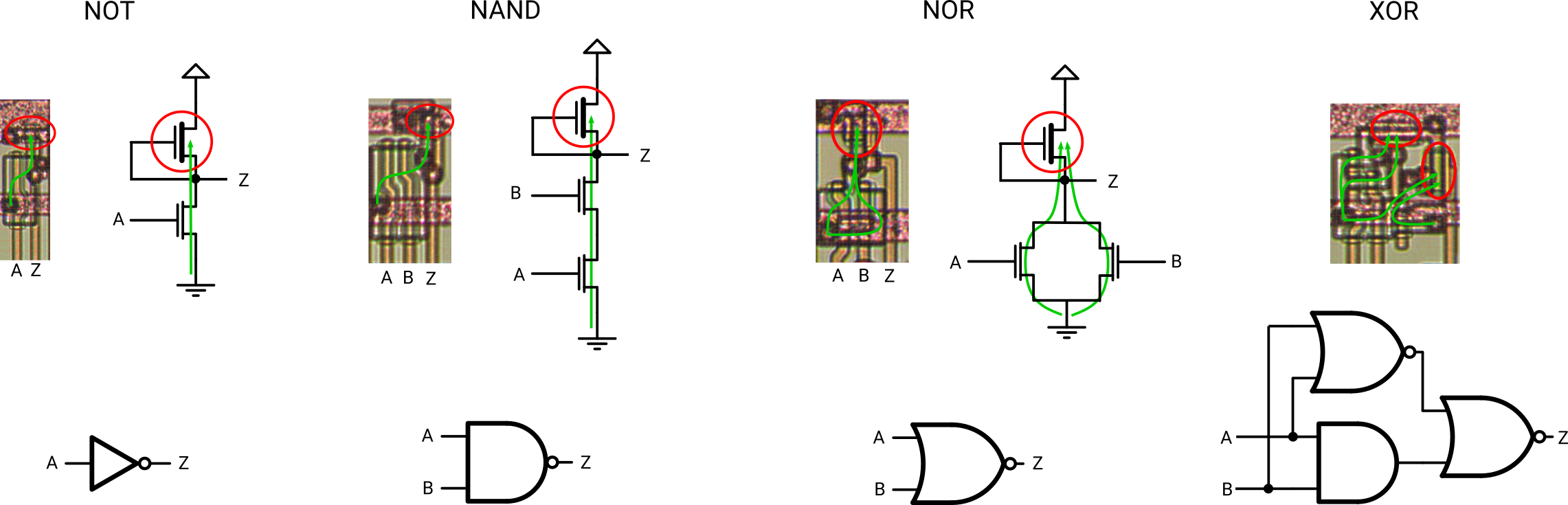
Tracing procedure applied to basic logic gates
The pull-up transistor acts as termination, so there must always exist one in a gate; not zero, not two, exactly one. It corresponds to the gate’s dot.
This aspect is important for tracing – the logic gate is incomplete without a pull-up.