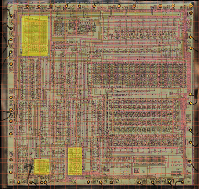
When I started to search for the random generator the first challenge was the decision where to begin with. Looking at the die, there are not many landmarks that provide clear guidance. The ROMs are quite prominent due to their regular structure, but they don’t have a direct relationship to the random generator. Furthermore, the purpose of two of the three ROMs was entirely unclear.
Next on the list of obvious items are the pads of course. They neatly follow the DIP40 pin-out and are assigned to functions in no time. Should I start off from the data or address bus? That would mean to dig through data paths whereas I expected the random generator to be located in a processing or calculation block. Somewhere in the middle between K-factors and final PCM output. With potentially deep logic cones on either side, not an appealing idea. I briefly considered entering the design via the few control pins, but the perspective to untangle piles of potentially complex control logic wasn’t appealing at all.
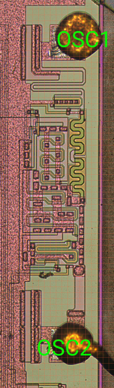 In the end I decided for tracing the clock tree first. That’s a single source signal, easy to identify from the pads, and – if Sanyo designed a reasonable clock system – fans out to all function blocks. I also hoped that the logic in the clock tree is less complex and that the purpose of such logic is easy to understand.
The OSC2 pin feeds directly into the clock generation system where the 3.58 MHz clock is divided by 2 before being used anywhere else. Identifying the divider was my first lesson in tracing logic from the die shot. After much back and forth I figured that all these polygons are just standard logic gates – and that they actually make sense. I mean, it’s located in the center of the die, and a /2 divider can be expected at the clock tree’s root.
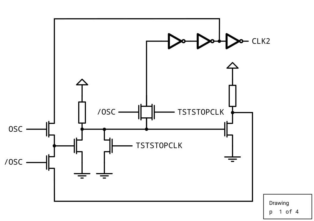
OSC2 /2 divider
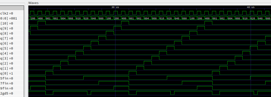
Curiosity was fueled enough to tackle further gates in the neighbourhood to the divider. This time I faced a number of flip-flops – they look different than the logic gates but once I understood the concept of 2-phase clocking and latch/feedback topology, they turned out to be positive edge triggered D-type registers arranged in a shift chain with feedback. Not too bad for starters, but isn’t that a bit too easy? Let’s build it a VHDL model and check the extracted circuit in simulation. The waveforms from simulation backed the extraction result: That shift chain generates 10+ staggered clocks.
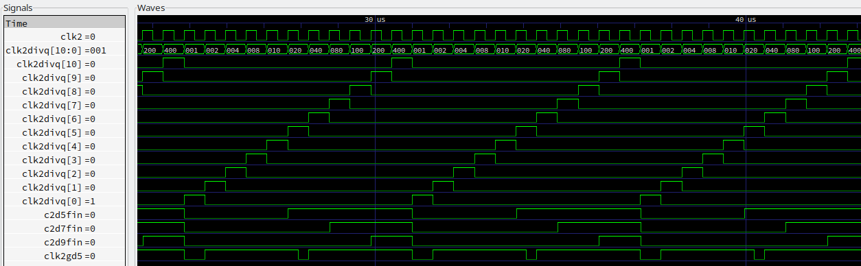
Core clocks of the VLM5030, clk2 is oscillator /2
Step by step I paved my way through the design (still searching for the random source):
- Extract the gates of a sub-circuit
- Reconstruct the sub-circuit as a VHDL model based on the extraction result
- Simulate the model to examine its behaviour and to validate the extraction
- Repeat with the next sub-circuit
At the point when the random source had been identified, I looked back at quite a collection of models running nicely in simulation. Should I stop here or keep on moving until I would hit a wall maybe?
TLDR; I decided to continue, repeatedly cycled through above steps and didn’t hit any walls. The VLM5030 gate-level replacement is available at FPGAArcade’s github repo.